-
Semiconductor Process
내용
◆ Semiconductor Process
Wafer, Glass를 Spin Cleaning, Develop, Etching 공정을 처리하는 설비
Photo Lithography Line - Wafer 8" & 12", Glass 210x210
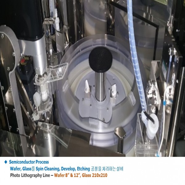
◆ Semiconductor Process
Wafer, Glass를 Spin Cleaning, Develop, Etching 공정을 처리하는 설비
Photo Lithography Line - Wafer 8" & 12", Glass 210x210